As I have recently got a PC/104 capable PC (VIA EDEN) I have thought about putting together a small Digital Input/Output (DIO) board for this. In my spare parts I have found some of the famous Intels 82C55 chips and in the internet I have found a quite good looking schematic.
 |
| http://technologyinterface.nmsu.edu/4_1/4_1s.html |
This kind of interface is a typical application of an ISA device - U1 - U3 are the buffers for the ISA interface, U7 is the address decoder and U9 - U10 generate the /CS signal for the 8255 for all the four addresses (8255 has four addresses - three for three 8 bit ports and one for control word). U10 seems to be a bit spare, so I decided to get rid of it and to add a switch for the address decode. Still it seems to be a bit complicated, but you really need all that glue logic to force it to work good. You can always interface it directly to the ISA, but this is highly unrecommended.

After having the complete schematic I started routing the board. So now the first problems emerged - It is really hard to fit all these ICs into PC/104 size format. Really, really hard. And not to mention to rout everything! so this is how it looks for now.
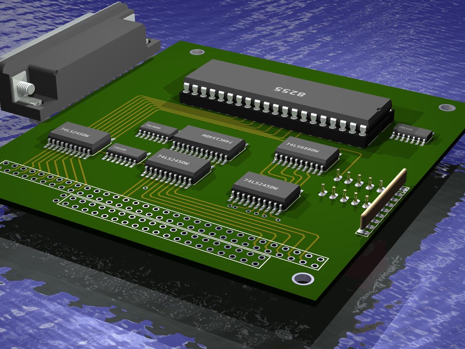
I have to redesign it completely I guess - rip-up every trace and start from scratch, as I have forgot to place the SUBD connector, and put everything into the same layer... this is not the best solution, especially when you are limited only to a double sided printed circuit board.
For sure I will post some more info when I finish redesigning the PCB.
Brak komentarzy:
Prześlij komentarz